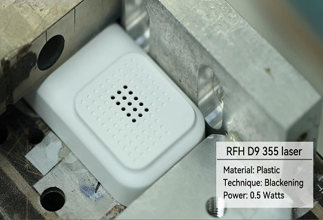
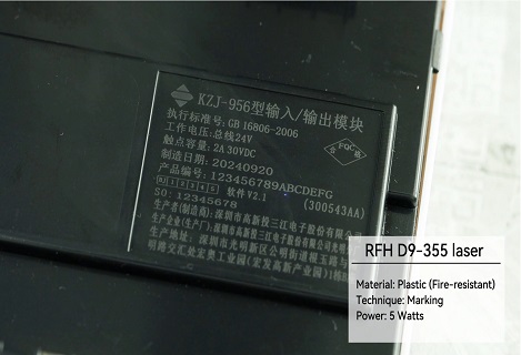
10W-15W uv laser

High Power UV Laser Marking in the Semiconductor Industry

Copper foil is a negative electrolytic material, a thin, continuous layer of metal foil deposited on the base layer of the circuit board, which acts as the conductor of the PCB. It easily adheres to the insulating layer, accepts the printed protective layer, and forms a circuit pattern after etching. Due to the small thickness of the copper foil, it is easy to lose balance or affect the accuracy due to relatively high impact or material, but the RFH 10w UV laser can solve this problem.

  • Laser Wavelength:

    354.7nm
  • Average Output Power :

    3W-10W @30kHz
  • Pulse Width:

    <12ns @ 30kHz
  • Pulse Repetition Rate :

    10-200kHz
  • Beam Quality (㎡) :

    <1.2
  • Beam Diameter :

    0.8±0.2mm Measured at window
  • Beam Full Divergence Angle :

    <2mrad
  • Beam Circularity :

    >90%
  • Pulse-to-Pulse Stability :

    <2% RMS/@30kHz
  • Average Power Stability :

    <5% RMS/8hr
  • Beam-Pointing Drift :

    <30μrad/℃
  • Polarization Ratio :

    >100:1
  • Polarization Orientation :

    Horizontal
  • Operating Temp. & RH :

    10℃ to 30℃ | <80%
  • Storage Temp. & RH) :

    -20℃ to 65℃ | <90 %
  • Electricity Requirement :

    100-240VAC |50/60Hz | Single phase
  • Power Consumption :

    <500W
  • Warranty :

    18months
  • Product Detail
  • Video

uv laser

High Power UV Laser Marking in the Semiconductor Industry

Semiconductor laser marking is a process that uses a laser marking system to mark semiconductor devices with identifying numbers, barcodes, or logos. The laser marking system directs a beam of high-energy light at the semiconductor device, which heats the surface of the device and causes it to change color. This change in color is used to create the markings that can provide part branding or traceability.


Semiconductor laser marking is an important part of the semiconductor manufacturing process, as it allows for the easy identification of semiconductor devices. In addition, semiconductor laser marking can be used for other purposes, such as part marking and barcoding.

Semiconductor manufacturing is the process used to create semiconductor devices, which are electronic components made from semiconductor materials. These materials are typically silicon-based, but can also be made from other materials such as germanium, gallium arsenide, or silicon-germanium. The parts are commonly used in computers, hand-held electronic devices such as mobile phones, tablets and electronic book readers, wearable devices and consumer electronics.


This manufacturing process starts with wafer fabrication, in which these materials are purified and shaped into thin disks called wafers. These wafers are then subjected to a series of complex processes that add electrical components such as transistors and other circuit elements. Also, many parts require laser marking before they are packaged and shipped to the customer.


Semiconductor manufacturing is a highly complex and precise process, and even small changes in the fabrication process can significantly impact the finished product's performance. That said, using precise and professional equipment is paramount, including the right semiconductor laser marking systems.


These laser marking machines are used to create semiconductor devices such as semiconductor chips, wafers, printed circuit boards (PCBs), integrated circuits (ICs), and other semiconductor devices.


Micro and 2D Code marking on IC Chips

Until recently, IC chips were only marked with lot codes. However, a growing need for encoded data has prompted many manufacturers to start using 2D codes.
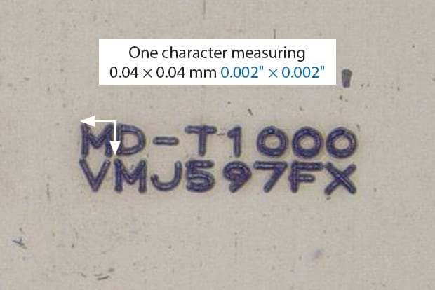
 

Micromarking


Laser markers have a very small beam spot, making them perfect for applications with a limited marking area. Micromarking - which is typically impossible for most systems - can be accomplished with the right laser. Various marking styles can also be selected, from shallow marking to deep engraving.
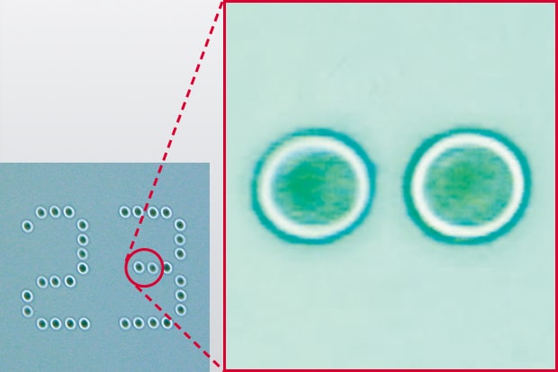
 

Marking silicon wafer


It's vital to keep surface damage to a minimum when marking a finished wafer, otherwise dust and debris can form. That's why UV and green lasers are the optimal wavelengths for these applications
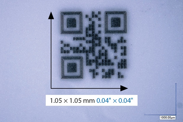
 

Marking LED ceramic package


Due to space limitations, ceramic packages often use 2D codes to contain all the necessary traceability information.

Plating and Coating IC Chip Removal

KEYENCE’s 3-Axis laser markers can mark the top surface of IC chips and remove plating or coatings within the same process. Since the laser accurately scans only along the edges of the IC, flash burrs over the leads can be removed without causing damage to the inside of the package.
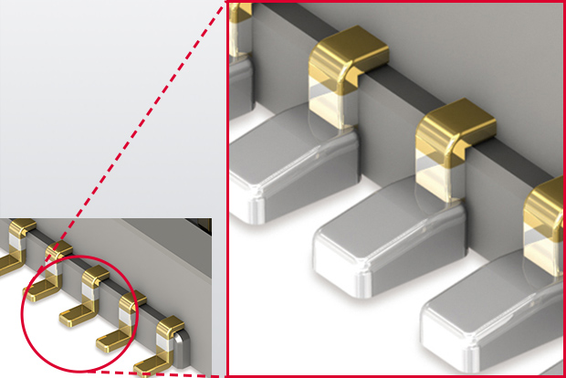
 

Removal of gold plating on terminals


To prevent solder wicking, lasers are used to remove the gold plating from connector terminals.
In the past, masks were used to avoid unnecessary plating. Today, connectors are designed smaller and thinner, and the pitches between the terminals are narrower. Consequently, it has become common practice to apply plating and then remove it with a laser for micron accuracy.
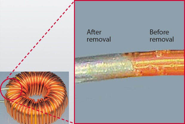
 

Removal thin-film coil coating


Previously, removers or edged tools were generally used to remove thin-film coating from coils. Now, laser markers have become useful because they require no consumables and ensure stable results.
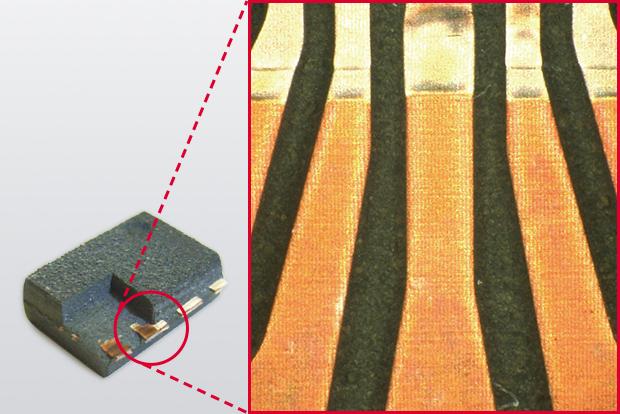
 

Resin coating removal


Chemicals are often used to remove resins on defective molds so that the molds can be analyzed. However, chemicals can damage the internal circuit and require multiple man-hours of work. Using a laser marker to remove resin saves running costs and time.
Leave A Message
If you are interested in our products and want to know more details,please leave a message here,we will reply you as soon as we can.
Related products
K-6 Integrated UV Laser 4W-6W
K-6 Integrated UV Laser 4W-6W-8W
K-6 series UV DPSS laser, developed and produced by RFH, covers 4W/6W/8W in laser power with short pulse width (<20ns@30K) ,superior beam quality (M²<1.2) and perfect laser spot quality (beam circularity >90%). K-6 series laser is ideal for high-end ultra-precise processing as well as marking in mobile phone shell , package of cosmetics, food, medicine and other high polymer materials, PCB, LCD, glassware surface, metal’s cladding material, plastic keypad, electronic component, gift, communication device, construction material and other areas.
Download datasheet
K-6 Integrated UV Laser 4W-6W
Why RFH UV laser is often used in laser marking plastic button switch?
Why RFH UV laser is often used in laser marking plastic button switch
Why RFH UV laser is often used in laser marking plastic button switch? More and more manufacturers choose UV laser marking machine to create pattern and characters on the plastic button switch. The focal spot of UV laser is pretty small with little heat transfer to surrounding material, so UV laser is also called “cold light source”. Because of this feature, heat effect won’t occur. Thus, distorting or burning of materials is no longer an issue.    Professional UV laser manufacturer - Shenzhen RFH Laser Technology Co.,Ltd    With 13 years of experience, the S9 series nanosecond UV laser developed and produced by RFH can engrave clear characters on the keyboard and the mouse. These kinds of characters can not only help people identify different buttons in the dark but also last long, for there are slightly protruding part on the buttons. This improves the durability and practicability of the keyboard and the mouse.   
Why RFH UV laser is often used in laser marking plastic button switch?
UV laser
UV laser featuring cold processing for marking plastic button on keyboard
 UV laser featuring cold processing for marking plastic button on keyboard More and more manufacturers choose UV laser marking machine to create pattern and characters on the plastic button switch. The focal spot of UV laser is pretty small with little heat transfer to surrounding material, so UV laser is also called “cold light source”. Because of this feature, heat effect won’t occur. Thus, distorting or burning of materials is no longer an issue.    Professional UV laser manufacturer - Shenzhen RFH Laser Technology Co.,Ltd    With 13 years of experience, the S9 series nanosecond UV laser developed and produced by RFH can engrave clear characters on the keyboard and the mouse. These kinds of characters can not only help people identify different buttons in the dark but also last long, for there are slightly protruding part on the buttons. This improves the durability and practicability of the keyboard and the mouse.   
UV laser
355nm UV laser
How can 355nm UV lasers be used in industrial production?
How can 355nm UV lasers be used in industrial production?   In modern industrial production, laser is an indispensable part. As the requirements for processing accuracy become more and more detailed, lasers are deeply involved in industrial links such as marking and cutting.
355nm UV laser
Laser engraving glass
Laser engraving glass, green laser or UV laser, which is better
Laser engraving glass, green laser or UV laser, which is better   At present, green lasers are widely used in the production of marking and engraving beer glasses, so many manufacturers have accelerated the promotion of production lines, and in fact, RFH UV lasers can also mark on glass.
Laser engraving glass
cuts diamonds
RFH 3W 5W 10W UV laser cuts diamonds, smooth without bursting
RFH 3W 5W 10W UV laser  cuts diamonds, smooth without bursting   Diamonds are one of the most high-end luxury goods. They are not only bright and look very bright, but also are one of the hardest substances in the world and have a very high collection value.
cuts diamonds
Marking Plastics
RFH 355nm UV Laser Cold Light Source Marking Plastics, No Carbonization, No Burning
RFH 355nm UV Laser Cold Light Source Marking Plastics, No Carbonization, No Burning   In the surface marking of plastics, there are always problems such as material being scorched, but the research and development of RFH 355nm UV laser has completely solved this problem, allowing more small and medium-sized growth enterprises whose main business is plastic marking to survive and room for development.
Marking Plastics
marking plastic auto parts
UV nanosecond laser marking plastic auto parts, accompany you to travel safely
UV nanosecond laser marking plastic auto parts, accompany you to travel safely   The development of automobiles has greatly facilitated human life, and the research and development of new energy vehicles has combined greenness and convenience. Plastic auto parts occupy an important position in the development and installation of automobiles, but the complex shape and a large number of demands make the marking of characters more complicated, and the RFH UV nanosecond laser can solve this problem very well.
marking plastic auto parts
Get the latest offers Subscribe for our newsletter

Please read on, stay posted, subscribe, and we welcome you to tell us what you think.

Leave A Message
Leave A Message
If you are interested in our products and want to know more details,please leave a message here,we will reply you as soon as we can.

Home

Products

About

contact