Latest Blog
Structuring of TCO/ITO Layers With the UV Laser 355nm-LaserMicronics
Apr 29 , 2023Structuring of TCO/ITO Layers With the UV Laser 355nm-LaserMicronics
Material-Friendly Laser Structuring of ITO Layers
ITO is a conductive material that is transparent in the visible wavelength range. It is applied in layer thicknesses ranging from a few tens of nanometers to a few hundreds of nanometers on glass or plastic films. The most commonly used process is sputtering. LaserMicronics does not offer coating services.
Most areas of application require structuring as a prerequisite. UV laser technology is the first choice for this too. Here, LaserMicronics uses a process that creates completely invisible insulation channels on the substrate surfaces by means of UV laser radiation.
Through the very high absorption of the UV laser radiation used, the ITO layer can be removed without the substrate material being damaged in the process. The laser generates extremely fine, invisible insulation channels less than 50 µm in width.
Applications for laser-structured TCO/ITO substrates are manifold and range from generation of conductive traces for display technology and sensors through thermal applications all the way to laboratory equipment and medical technology applications.
Do you require TCO/ITO structuring support? We can help you find the solution for your individual requirements!
Advantages of Laser Structuring of TCO/ITO Layers
Absolutely invisible structuring of transparent ITO coatings
No damage to the substrate material
Flexibility: Layout can be changed at any time
Structuring directly from CAD data
Reduction of technological steps (no resist application, no etching)
Ultrafine structures with <50 µm traces/spaces possible
High positioning accuracy through registration of fiducial marks or other visible marks
Today,we will recommend you RFH UV laser brand from China.
20watt high power uv laser source cutting ceramics
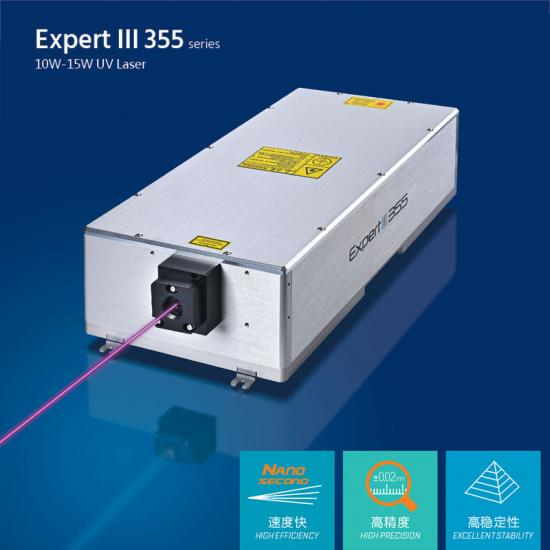
Expert III 355 series UV DPSS laser, developed and produced by RFH, covers 10w-15w in laser power with short pulse width (<20ns@40K) ,superior beam quality (M²<1.2) and perfect laser spot quality (beam circularity >90%). It is widely used in PE/PCB/FPC cutting, glass & sapphire cutting, drilling, scribing & cutting used in high precision micromaching areas.
