Latest Blog
532nm green laser for silicon wafer microvias and blind holes
Jul 06 , 2023The Prowess of the 532nm Green Laser: Illuminating the World of Silicon Wafer Microvias and Blind Holes

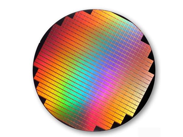
In the realm of silicon wafer fabrication, precision and ingenuity reign supreme. As the demand for smaller, more intricate circuits continues to surge, the process of creating microvias and blind holes becomes an art form that requires a touch of brilliance. Enter the remarkable 532nm green laser, a trailblazer among technologies, poised to revolutionize the world of silicon wafer processing.
Harnessing the captivating power of green light, this exceptional laser source unfurls an artistic tapestry of finesse and accuracy upon the silicon wafer canvas. Operating at a wavelength of 532nm, it encapsulates a realm where advanced engineering meets harmonized aesthetics, delivering unparalleled results in the world of silicon wafer fabrication.
First and foremost, the 532nm green laser bewitches with its capacity for immaculate precision. As the laser beam delicately touches the silicon wafer's surface, it dances across the intricate landscape with controlled grace, manifesting precise microvias and blind holes. With each pulse of its vibrant green energy, it etches a signature of ingenuity onto the silicon wafer, ensuring minute details and precise circuitry are flawlessly preserved. The transformative power of this laser source lies not only in its ability to create, but to elevate creation to an art form, transcending functional necessity to breathe life and expression into each silicon wafer.
Silicon wafers, by their very nature, demand adaptability and versatility. Their complex structures require microvias and blind holes that harmonize with their form without compromising performance. Herein lies the brilliance of the 532nm green laser. With its astute finesse, it maneuvers seamlessly, creating precise microvias and blind holes on the silicon wafer effortlessly, matching the wafer's contours with meticulous accuracy. Whether it be interconnects, through-holes, or intricate patterns, this laser source ensures that each element is etched onto the silicon wafer with unrivaled grace, preserving the integrity and functionality of the circuitry.
Beyond its inherent precision, the 532nm green laser represents an epochal moment for the silicon wafer industry in terms of sustainability and efficiency. With factors like shrinking product lifecycles and increasing environmental consciousness taking center stage, manufacturers seek innovative solutions that minimize waste and reduce their carbon footprint. This laser source, with its impeccable accuracy and controlled energy output, achieves an optimal balance between precision and sustainability. By minimizing material removal and energy consumption, it empowers manufacturers to not only produce exquisite silicon wafers but also contribute to a greener future.
Furthermore, the versatility of the 532nm green laser extends beyond microvias and blind holes. Its radiant green energy illuminates a path toward new possibilities in the realm of silicon wafer processing. From precise cutting and drilling to selective ablation and etching, this laser source's capabilities transcend the ordinary, delivering exceptional results that redefine the boundaries of innovation. As manufacturers delve into the extraordinary potential it offers, the 532nm green laser becomes a catalyst for ingenuity and a hallmark of cutting-edge silicon wafer production.
As we marvel at the prowess of the 532nm green laser, we witness a transformation in the world of silicon wafer processing. Its radiant touch, guided by precise engineering and a deep understanding of the industry's demands, sets a new standard for excellence. With each silicon wafer it encounters, this laser source whispers tales of innovation, sustainability, and progress, carving a path toward a future where precision and aesthetics unite seamlessly.
In the symphony of silicon wafer production, let us embrace the transformative power of the 532nm green laser. Together, we embark on a journey of precision, sustainability, and boundless creativity, where each silicon wafer stands as a testament to the remarkable fusion of artistry and technological advancement. Shedding light on the world of microvias and blind holes, this laser source guides us toward a realm where possibilities are limitless and perfection is unrivaled.